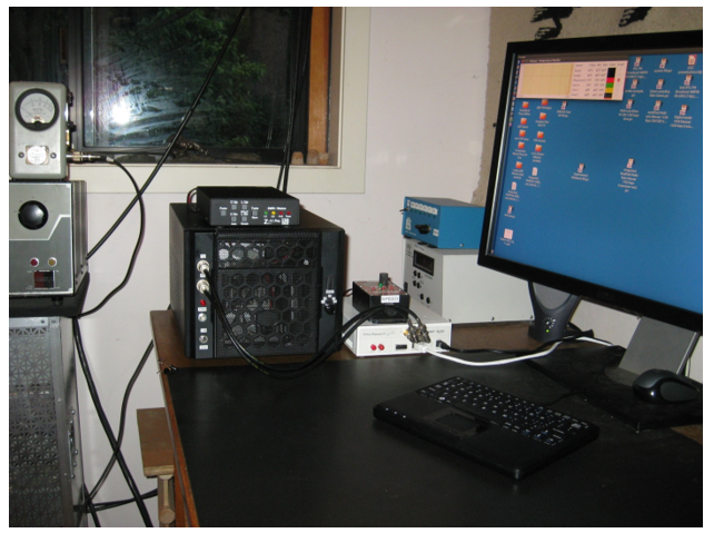
For the ham radio enthusiast, the acid test of an SDR / DSP transceiver design is to use that radio design to communicate with other hams over the air. My latest projects have been to package all the necessary components for separate transceiver interfaces for the HF (3 to 30 MHz) and the VHF (50 MHz to 6 GHz) portions of the spectrum. Through these interfaces, I can connect my SDR to suitable antennas and make on the air contacts. The most recent example, the complete HF interface unit, is packaged in a tidy miniATX computer case depicted in the photo. I will outline a practical HF interface design as a concept.
Any SDR interface to the real radio world is completely analog in design. The interface with the real world starts with the antenna input. A user-controlled switch directs the antenna connection either to the transmit or to the receive signal path. Each signal path follows a distinctly different route through the interface. The receiver path in the native SDR board is ‘wide open’ with no RF filtering. The SDR wide-band A/D converter is subject to the cumulative RF energy from all signals at all frequencies that the antenna captures. For HF, the receive signal path begins at the antenna input and continues into a high pass filter. This filter reduces the potential signal overload from powerful stations in the local AM broadcast band. Following the receive filter, a preamplifier with sufficient gain and low enough noise figure amplifies the input signals so that local background noise from the antenna is the limiting factor in receiver sensitivity. The preamplifier is generally necessary for sufficient receiver sensitivity at the higher HF frequencies such as 21 and 28 MHz. The receive RF interface chain connections to the receiver input of the SDR front end. The transmit signal path begins at the transmit output connection from the SDR front end. That SDR generated analog output passes through solid state amplifiers with sufficient gain to generate a signal of sufficient power for communication purposes: a typical RF output of between 10 and 100 watts for practical HF communications. At the end of the amplifier chain, and before the antenna switch, is a low pass filter system. This filter is designed to meet the FCC requirements for harmonic suppression of the transmitted signal. The complete transmit chain terminates at the antenna switch. Linking all the elements together is a suitable power supply and internal control links that actuate the antenna switch and the amplifier modules as necessary.
The essential backbone of the any SDR real world RF interface are the amplifiers for receive and transmit signal paths. Amplification of both signal paths is essential for satisfying on the air operation. The available SDR receiver front ends have varying degrees of useful sensitivity and noise figure. Ettus USRP series for HF and VHF exhibit a relatively high receive noise figure and no low noise preamplifier. Similarly, transmitting SDR front ends provide low output levels, in the milliwatt range for the USRP anywhere in the spectrum. Attention to these amplifier needs is essential in the design. Finding RF transmit amplifiers with sufficient gain and enough power capacity was the main challenge with these interfaces.
The RF interface is simple in concept, but as always, there is a devil in the details. Obtaining the parts is not too difficult, but not without cost. Most of the modules: high and low pass filters, and the receive preamplifier are off the shelf items: www.minicircuits.com. An HF transmit amplifier can be purchased as a kits from many sources. The remainder of the components such as the power supply and the antenna relay are commodity items available from the Internet. The packaging for my interfaces, small computer cases, is only one of many potential solutions.
It is satisfying to use both of the real world interfaces to communicate with ham friends, and as a useful proof of concept tool for my SDR designs. Having these units together and working well clears up needed space at my busy GNU Radio workstation. Receiver input and transmitter output connectors, filter band switch and a single power switch. Doesn’t get any more user friendly.
Link to Terms and Abbreviations: Terms and Abbreviations
Link to Home Page: Home Page